IR2125 Introduction
The IR2125 is a high-voltage, high-speed driver for power MOSFETs and IGBTs with over-current protection. It supports logic inputs down to 2.5V and features a robust HVIC and CMOS design. With a 500V max offset, 12-18V output, and 150ns typical switching times, it delivers high pulse current with minimal cross-conduction. The driver includes cycle-by-cycle over-current shutdown, configurable via an external capacitor, and can drive N-channel MOSFETs or IGBTs in high- or low-side configurations up to 500V.
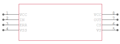
IR2125 Symbol

IR2125 Footprint

IR2125 3D Model

IR2125 Pinout

VCC: Logic and gate drive supply
IN: Logic input for gate driver output (HO), in phase with HO
ERR: Serves multiple functions; status reporting, linear mode timing and cycle by cycle logic shutdown
COM: Logic ground
VS: High side floating supply return
CS: Current sense input to current sense comparator
VB: High side floating supply
HO: High side gate drive output
IR2125 Typical Connection

IR2125 Block Diagram

IR2125 Specification
| Parameter | Specification |
| Gate Type | IGBT, N-Channel MOSFET |
| Supply Voltage | 0V ~ 18V |
| Logic Voltage | 0.8V, 2.2V |
| Peak Output Current(Source, Sink) | 1.6A, 3.3A |
| High Side Voltage | 500 V |
| Rise / Fall Time (Typ) | 43ns, 26ns |
| Operating Temperature | -40°C ~ 150°C |
| Package | 8-PDIP |
| Channel Configuration | Single-channel |
IR2125 Features
Floating channel designed for bootstrap operation
Fully operational to +500V
Tolerant to negative transient voltage
dV/dt immune
Gate drive supply ranges from 12 to 18V
Undervoltage lockout
Current detection and limiting loop to limit driven power transistor current
Error lead indicates fault conditions and programs shutdown time
Output in phase with input
2.5V, 5V and 15V input logic compatible
Also available LEAD-Free
IR2125 Applications
Switching Power Supplies
Motor Control
DC-DC Converters
Inverters
Induction Heating
UPS Systems
Battery Chargers
Renewable Energy Systems
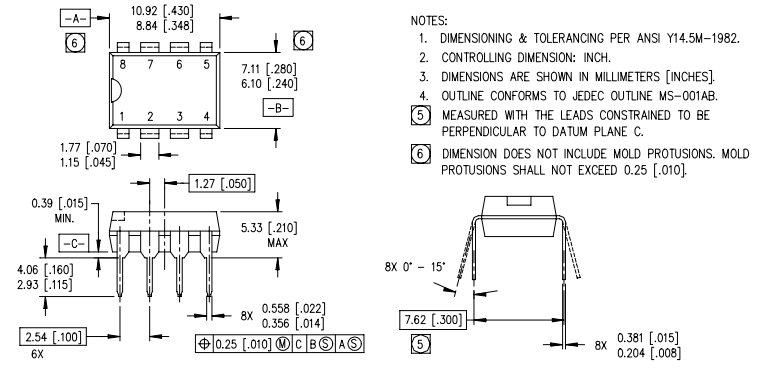
IR2125 Package
The IR2125 is available in an 8-PDIP configuration, designed for through-hole mounting. This package is durable, compact, and offers reliable electrical insulation, making it ideal for a wide range of applications. With a standard pin pitch of 2.54 mm and a total width of 7.62 mm, it ensures compatibility with common PCB layouts.
The package dimensions include a length of 9.81–10.16 mm, a height of 4.06–5.33 mm, and pin lengths of 2.92–3.43 mm. Its thermal resistance is approximately 80°C/W, providing adequate heat dissipation for efficient performance in typical operating environments. This 8-PDIP package is suitable for designs requiring robust and easy-to-solder components.

How to Use IR2125?
When using the IR2125, proper pin connections are essential. Connect the VCC pin to an appropriate logic power supply and ensure that COM is grounded. The high-side floating supply pins VB and VS require bypassing with a suitable capacitor. The logic input IN controls the output at the HO pin, and the input signal must meet the required logic level specifications.
For over-current protection, connect the load current signal to the CS pin via a shunt resistor. When the current exceeds the set threshold, the IR2125 activates its protection function, limiting the gate drive voltage and setting the shutdown time based on the value of the external capacitor. Finally, connect the HO pin to the high-side power MOSFET or IGBT to deliver the gate drive signal.
FAQs
What type of device can the IR2125 drive?
The IR2125 is designed to drive N-channel power MOSFETs or IGBTs in high- or low-side configurations.
How does IR2125 provide over-current protection?
The IR2125 features a current sense comparator connected to the CS pin. When the load current exceeds the set threshold, the driver limits the gate voltage and initiates a cycle-by-cycle shutdown based on an external capacitor.
What are common applications for the IR2125?
The IR2125 is commonly used in motor drives, switch-mode power supplies, and uninterruptible power systems (UPS).