The MAX5888 is an advanced 16-bit 500Msps digital-to-analog converter (DAC) designed to meet the demanding performance requirements for signal synthesis applications in wireless base stations and other communications applications. The converter is available in a 68-lead QFN package with exposed blades (EP) for extended industrial temperature ranges (-40°C to +85°C).
Running from a single 3.3V power supply, this DAC provides excellent dynamic performance, such as 76dBc spury-free dynamic range (SFDR) at fOUT = 40MHz. The update rate of 500Msps is supported, and the power consumption is only 250mW. The MAX5888 uses a current steering architecture that supports a full range of output currents from 2mA to 20mA and allows differential output voltage swings between 0.1VP-P and 1 vp-p.
The MAX5888 integrates a 1.2V bandgap reference and control amplifier to ensure high precision and low noise performance. In addition, a separate reference input pin enables the user to apply an external reference source for optimal flexibility and improved gain accuracy, and its digital and clock inputs are designed for differential low-voltage differential signal (LVDS) compatible voltage levels.
MAX5888 Pin Configuration

Simplified MAX5888 Block Diagram

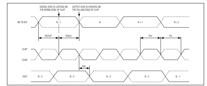
Detailed time relationship

MAX5888 Features and Applications
● 500Msps Output Update Rate
● Single 3.3V Supply Operation
● Excellent SFDR and IMD Performance
- SFDR = 76dBc at fOUT = 40MHz (to Nyquist)
- IMD = -85dBc at fOUT = 10MHz
- ACLR = 73dB at fOUT = 61MHz
● 2mA to 20mA Full Scale Output Current. ♦ 2ma to 20ma full scale output current
● Differential, LVDS-Compatible Digital and Clock inputs
● On-Chip 1.2V Bandgap Reference
● Low 130mW Power Dissipation
● 68-Lead QFN-EP Package
Applications
● Base station: Single/multi-carrier UMTS,CDMA, GSM
● Communication :LMDS, MMDS, point-to-point microwave
● Digital signal synthesis
● Automated test equipment (ATE)
● Instrument